What are Micro-LEDs?
Micro-LEDs represent a paradigm shift in display technology, offering unparalleled brightness, contrast, and energy efficiency. We understand the intricate complexities of these miniature light sources, and our advanced analytical tools provide the precision needed to characterize and optimize their performance.
Our solutions delve into the core of micro-LED technology, enabling:
By providing comprehensive analytical solutions, we empower researchers and manufacturers to push the boundaries of micro-LED technology, driving innovation in displays, lighting, and beyond.
Micro-LEDs are a revolutionary display technology that utilizes arrays of microscopic light-emitting diodes to create images. Unlike traditional LCDs that rely on backlighting, or OLEDs that use organic materials, micro-LEDs are self-emissive, meaning each individual LED pixel produces its own light.
Key characteristics of micro-LEDs include:
These unique properties make micro-LEDs a promising technology for a wide range of applications, including:
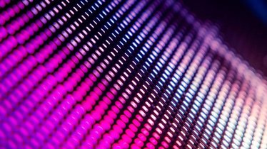
Spectroscopic characterization and detection of yield-killing defects in micro-LED wafers
Emerging display technologies demand high brightness, low power consumption and longer lifetime. Arrays, of self-emitting, micron-sized LEDs or Micro-LED (µLED), are considered a strong contender to replace current OLED or LCD displays. The estimated growth of the micro-LED (µLED) market is USD 21 billion by 2028. Increasing demand for brighter & more power-efficient displays in automotive panels, smartwatches, mobile devices are some of the factors driving the growth of the segment.
Despite the huge potential, µLED technology is not yet fully commercialized. This is mainly due to the cost and challenges involved in the production process. For example, wearable devices, such as smart watches or augmented reality (AR) glasses, demand high resolution or high pixel density. To achieve high pixel density, the size of the µLEDs should go down to 3 µm or lower. At this length scale transferring the dies to the wafer and improving the yield is challenging, Low yields can drastically increase production costs.
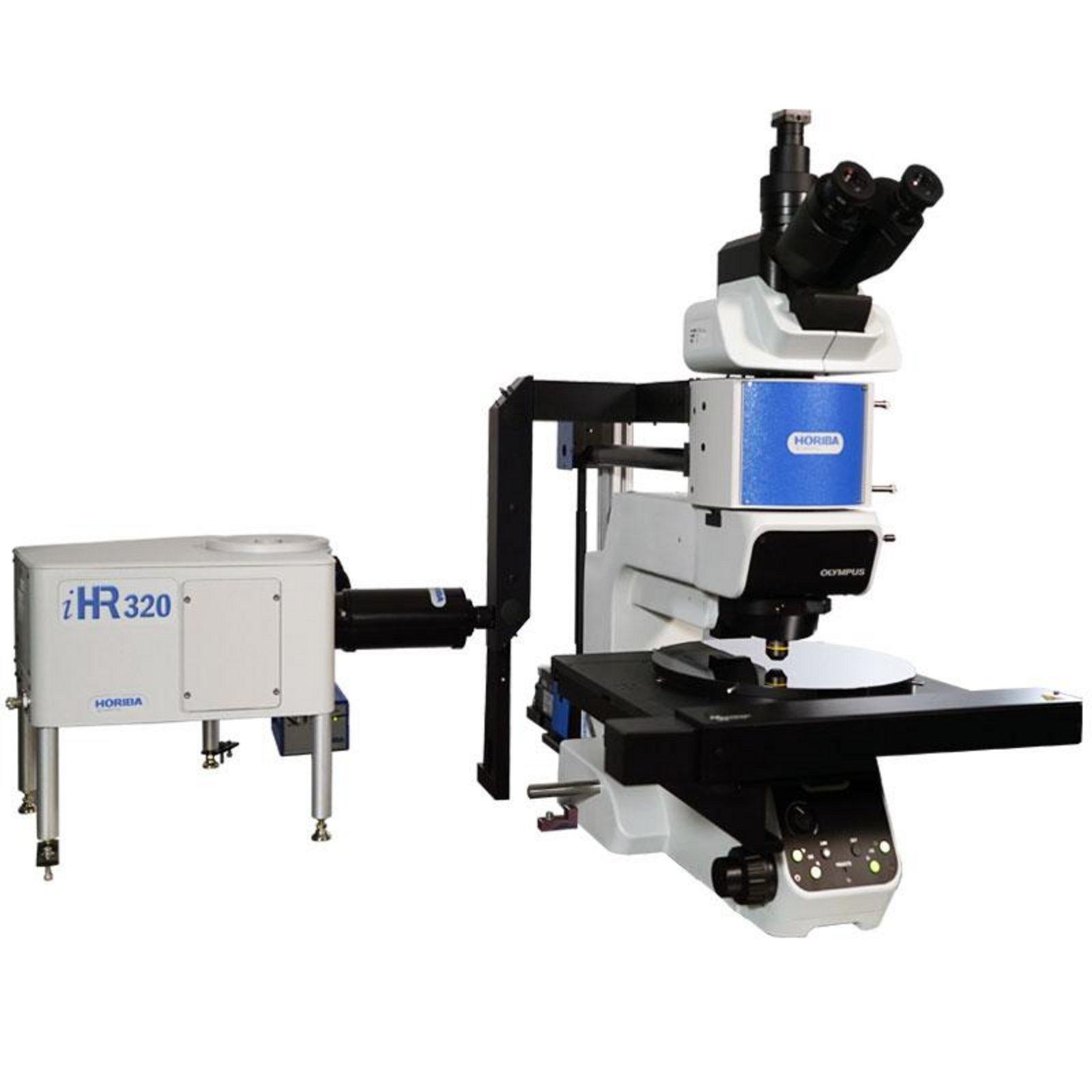
Standard Microscope Spectroscopy Systems
With its unique set of accessories, the SMS family of systems enable any standard microscope to be fitted with a spectrometer and a detector, offering the ability to perform techniques such as:
Do you have any questions or requests? Use this form to contact our specialists.